Sunday, January 24, 2016

Inside the arm1v - the ALU control logic

This is one of a number of posts on my work on reverse engineering the armv1 processor.  The first in the series, and an index of the other articles can be found here.

My first post in this series described in some detail a one-bit slice of the ALU, and identified quite a number of control signals that feed all 32 bit slices which determine how the ALU operates. Now that I've reverse-engineered the overall instruction decoding and sequencing mechanism we now have enough context to make a start on reverse-engineering the circuitry that generates the ALU's control signals. This turns out to be more complex than I first expected and a full understanding of what's happening will probably have to wait until other parts of the processor have also been reverse-engineered.

Let's make a start by setting the context. The ALU circuit from my earlier post is reproduced below; we'll need to refer to it as we proceed.


The location of this circuitry, and it's control circuitry, on the silicon are as follows:


Let's now zoom in on the ALU control area:


The ALU Control Logic comprises two distinct areas - (1) a bunch of "ad-hoc" gates and drivers sitting just above the ALU itself, and (2) just above them, a Programmable Logic Array which is referred to as PLA-1 in an earlier blog. In the same area is the logic which implements the Program Status Register which is not discussed here.

The overall circuit is as follows:


The circuit diagram is laid out roughly as it is in the silicon - a bunch of control signals come in from above and feed PLA-1; the buffered PLA-1 outputs, and a couple of outputs from the instruction-decoder, then feed downwards to provide the control signals to all 32 bit slices that form the ALU. Not surprisingly, these control signals tally exactly with the signals in the ALU circuit at the beginning of this blog.

The Carry Logic on the left (highlighted in blue) feeds the Carry bit from the PSR Logic (node 8083) to bit 0 of the ALU. The Carry bit is delayed by a single clock cycle using a dynamic latch (I've used a D latch symbol for ease of drawing) and conditioned by two outputs of the PLA as per the following truth table:

This shows that the PLA-1 outputs can either pass the Carry bit straight to bit 0 of the ALU, or force the Carry line to be either 0 or 1.

The Dynamic Register Control circuitry on the RHS (highlighted in orange) shows that the two dynamic latches in the ALU (one on each operand path) are controlled by outputs on PLA-2 (the instruction decoder), with latching occurring on the trailing edge of the Phase 1 clock. the Operand 1 latch is also operated one clock cycle after the PLA-2 signals (8062, 8061, 8060) are all simultaneously low. We'll try to make sense of the purpose of this part of the circuit later.

PLA-1 Content - Input Decoding

After all this context setting it's now time to look at what's in PLA-1. The PLA layout is very similar to the instruction decoder PLA-2 described earlier:


The 8 input selection signals enter the PLA from the lower right and the signals, and their inverted versions, feed 16x vertical columns. Which transistors are fitted (or missing) determine which one of the 31 rows within the PLA is selected. There are further details about the operation of this circuit in the earlier blog post.

Let's start with the row selection logic on the RHS of the PLA, a raw dump of which is below (with the top row of the table corresponding to the top row in the PLA):


The content displayed in this format doesn't give us much insight into what is happening. However, after a little study the following pattern emerges:

It becomes clearer that the 3x inputs from PLA-2 (8062, 8061, 8060) form a "command" that narrows down which row will be selected. (Note that I've shown these 3x signals in the order that they enter PLA-1; similarly the earlier description shows these signals in the order that they exit PLA-2 - but they are in a different order! This is the way the chip is wired! So you need to remember to swap the bit ordering when you compare the data between the two PLAs!)

Let's start by looking closer at the first command: "111" from PLA-2, which narrows the selection to rows 15-30. If we refer to the PLA-2 logic table & find which rows generate a "111" (remembering to reverse the bits, which happens to not matter in this case), we find it appears on three rows: 1, 3, and 4 (highlighted in light blue).


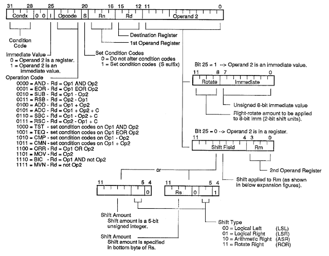
All three rows are associated with the last (or only) cycle of a DP (Data Processing) instruction. So, returning to the PLA-1 table above, the signals on the Instruction Bus b24 to b21 are from a DP instruction. The DP instruction format is:


And, as expected, we see that b24 to b21 correspond to the "Operation Code" - AND, OR, etc. So we can conclude that rows 15 to 30 of PLA-1 correspond to each ALU operation.

By following a similar process and taking each of the remaining commands in turn we can gain some understanding of what rows 0..14 are for. However this analysis reveals lots of specific details - there is a lot of complexity here. The annotated PLA-1 row-selection table is as follows:


What's clear from this table is that the ALU is being used for a lot more than the DP instructions that are visible to the programmer - almost half of this table is for other purposes! In the main the use of Instruction Register bits 24..21 makes sense given the context. The one exception is for command "000" (rows 0, 1 above); the Instruction Register bits are only valid & meaningful on a couple of the 9 rows this command is used. I suspect that this command is sometimes used as a "no-op".

We can also perhaps gain some insight into what the signal "From Trap Ctrl (8158)" is. It only influences the row decoding for rows 6, 7 which is associated with LDR and LDM instruction execution. We know from the instruction descriptions that there are special rules in cases where a data fetch abort occurs:

  • for the LDR instruction: "The data fetch may abort, and in this case, the base and destination modifications are prevented", 
  • for the LDM instruction: "If an abort occurs...the final cycle is altered to restore the modified base register") 

Perhaps this logic is to implement this functionality?

PLA-1 Content - Output Values

Now that we've made an initial analysis of the input decoding, it's time to see what sense we can make of the output values. The table below is laid out to reflect the physical layout and therefore shows the output values on the LHS. There are also some notes on the left.


There is an awful lot of information contained in this table!

Let's start with the DP rows - 15 to 30:

  • The good news is that on rearranging the order of the 6 right-most output columns, these values exactly correspond to the table that appeared in my first post on the ALU! Whew!
  • If we now look at the output columns for 8087, 8088, we know from the earlier circuit diagram that these values determine what signal is fed to the Carry In on bit 0 of the ALU. And we only need to look at those rows where the output signal "/Enable C chain" (8116) is 0 (since the Carry signal is ignored otherwise). The comments on the left captures the results. The Carry In signal is set to exactly the values we would expect for associated op-code.


  • The first output, "To INST SKIP logic (8065)" is interesting in that it is only zero for the 4x comparison op-codes. About these op-codes the documentation states: "They are used only to perform tests and to set the condition codes on the result, and therefore should always have the S bit set" (we can see from the DP instruction format above that the S bit is defined as "Set Condition Code", 0 = Do not alter condition codes, 1 = Set condition codes). I suspect that this output from the PLA is used by the INST SKIP logic to detect if this is an invalid instruction.
  • The output "To PSR Logic (8064)" appears to control when the PSR is updated. Since 8064 is high for all the DP op-codes, and low for all other ALU operations, it probably controls when the Carry, Overflow, Negative, and Zero flag can be updated (subject of course to the S bit, as described earlier). 
  • The output "To PSR Logic (8059)"  is only high when an arithmetic operation (as opposed to a logical operation) is taking place. It therefore selects where the Carry flag is updated from - either the ALU output, or the result of the shift operation, and whether the Overflow flag is updated or not. See p2-32 of the VTI arm data book (1990) for a more complete description of the rules regarding how the PSR bits are updated.

Now that we've completed analysing the DP instructions, let's move the remainder of the table - rows 0 to 14.

To analyse rows 0 to 14 of the PLA-1 output table I assumed that the ALU would be carrying out similar operations to the DP instructions we've already been looking at. I therefore expected to see the same output settings on these rows as the rows we've already analysed. The results of this comparison work are shown in the Notes on the left of the table above. A summary is:

  • Matches: There are 8 rows with exact matches, and select a variety of ALU op-codes: MOV, ADD, SUB, RSB (reverse substract).
  • Variants: A further 5 rows match, apart from the Carry In selection. These are described further below.
  • Unknowns: Two rows have identical values, but don't match any DP instruction.
Let's look further at the variants. Although they appear on 5 rows, there are just two versions:
  • ADD (but Cin = 1). The normal ADD has a Cin = 0, so this variant has the result = Op1 + Op2 + 1 (where Op1 and Ap2 are the two operands presented to the ALU).
  • RSB (but Cin = 0).  The normal RSB has a Cin = 1, so this variant has the result = Op2 - Op1 - 1. 
We can make educated guesses as to what is happening on each of these rows. For instance, on row 2, we are executing a Branch or Branch and Link instruction, and are almost certainly calculating the destination address by adding the PC to the PC-relative offset which appears within the instruction  (we've seen in an earlier article how there is logic in the Read Bus B that extracts the 24 bit offset).

Conclusion

It turns out that the ALU control logic is more complex than I expected. What is clear is that the chip designers really maximised the use of the ALU! 

Whilst I've completely reverse-engineered the control circuitry, I've only made a start on unraveling what is actually going on. A full understanding requires some more analysis of the circuitry itself, and on getting a wider view on what is happening elsewhere on the chip. My list of "to-do" items includes:
  1. What exactly is the "unknown" ALU command we discovered above?
  2. What values appear at the inputs to the ALU (Operand 1 and operand 2) for each of the rows above (this requires other parts of the processor to be reverse-engineering first). This will also give us a better understanding of why the variants to the ADD, RSB opcodes are introduced.
  3. What exactly is being latched into the ALU's dynamic registers, and what is the sequencing associated with this? And why does the circuit above have the specific logic to introduce a one cycle delay for when DP instructions are executed?


Monday, January 18, 2016

Inside the armv1 - decoding barrel-shifter commands

This is one of a number of posts on my work on reverse engineering the armv1 processor.  The first in the series, and an index of the other articles can be found here.

Today I'm going to solve a puzzle I have been pondering for some time - how the processor implements instructions that reference 4 registers.

If we look at the data processing (DP) instruction format in more detail, we see that there are the following instruction types:

If we set Bit 15 to zero (Operand 2 in a register), and Bit 4 to one (Shift amount in a register) we get the following layout (made from copying/pasting portions of the image above):


This layout plainly shows this this single instruction references 4 registers simultaneously - Rd (the destination register), Rn (one of the ALU operands), Rm (the second ALU operand), and Rs (which gives the amount by which Rm is first shifted).

However various architecture descriptions of the arm's Data Processing instructions only refer to there being two input operands and one output register. This matches the descriptions of two data read buses (referred to as "Bus A" and "Bus B" or "read bus A" and "read bus B"), and also matches there being just 3 sets of register select logic (which was explored in detail in an earlier post). So how does the processor execute an instruction which references 4 registers?

A clue to solving this mystery was in my last post, where I analysed how the instruction decoder works. By referencing the first table in that post we see that the instruction decoder treats as a special case all Data Processing instructions where the shift amount is in a register. These instructions execute in 2 cycles, one more cycle that all other Data Processing instructions. It would be safe to bet that the first cycle extracts the shift amount from the Rs register and holds the value somewhere, and on the second cycle actually carries out the ALU operation.

Let's now move to the processor itself to verify that our guess is correct. The area of the chip that we're interested in is highlighted in red below. Ken Shirriff has already given an overview of how the barrel shifter works here:


If we zoom in a little further, we see that there are two distinct sections in this area:


The lower area generates the column drive signals to the barrel shifter itself. The shift-amount and shift-type is via signals originating in the upper "Barrel Shifter Decode Selection" logic. We won't look at the driver logic in any further detail in this post. Instead we turn to the upper section, and start by zooming in some more:


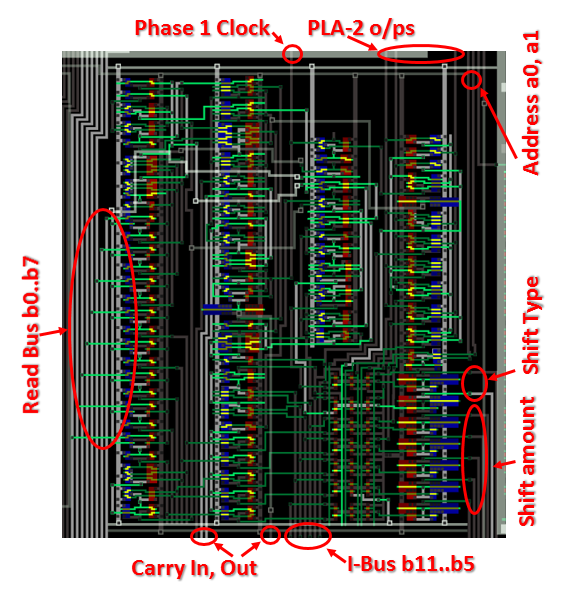
The layout of this upper section is spectacular in that all the inputs and outputs to the logic are very readily apparent, and are marked on the diagram:

  • The I-Bus inputs b11..b5 correspond to the Shift Amount (b11..b7) and Shift Type (b6..b5) that we saw in the instruction layout we looked at above. 
  • The outputs on the RHS - Shift Amount (5 bits) and Shift Type (2 bits) are the signals that feed the Barrel Shifter Driver Logic that we saw earlier. 
  • The 3x outputs from the PLA (nodes 8287, 8288, b286) that enter the area from above correspond to columns 2, 3, 4 of the PLA output table I included in my last blog.
  • Two signals derived from the lowest two address outputs lines enter the area from above and to the right.
  • 4x signals associated with Carry processing enter/exit from the lower edge.
The main logic areas are also apparent:


We've found the 8-bit wide dynamic latch that stores the register-sourced shift-amount from the Read Bus!

The other key logic is the group of seven 6-way multiplexers, whose outputs feed via the seven drivers to the rest of the barrel-shifter logic.

The 3 to 8 decoder is driven from the 3x PLA outputs (nodes 8287, 8288, b286) and 6 of its outputs select which of the 6-way multiplexer inputs is chosen. A further output controls the Dynamic latch, and the final 3 to 8 decoder output is not implemented.

The remaining logic that is not highlighted in the diagram is complex and convoluted; it's task is to ensure that the correct shift results occur, even when a shift amount greater than 32 is selected. This includes ensuring that the Carry bit is set appropriately and that the sign bit is extended in the correct manner. The rules are described on page 2-34 of the VTI arm databook (1990). I won't dwell further on this part of the circuit.

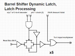
The dynamic latch circuitry and associated latch processing is straightforward:


The data on the Read Bus is latched during phase 1 of the clock only when output 7 of the 3-to-8 decoder has been selected (i.e. all 3x inputs from the PLA are high). The latched data (or zero) is then available on one of the 6 inputs to the multiplexer. Zero is selected depending on the complex logic referred to earlier.

The output driver circuitry for each of the 7 signals is just two inverters in series.

The multiplexer circuitry, and decoding circuitry, is identical in form to the read bus input multiplexer I described in my earlier blog on register selection, and won't be repeated here.

Just the following "glue logic" circuits generate additional inputs to the multiplexer:


Note how the Shift Type in I-Reg b6 and I-Reg b5 are potentially adjusted, dependent on complex logic, in a similar manner to how the shift-amount described earlier might be adjusted.

The table below summarises the multiplexer's operation, and lists what the 7x outputs to the Barrel Shift Driver Logic are for each of the 8 combinations on the 3 signals from the PLA.


If we compare these PLA values, and the barrel-shifter outputs, with the values in the PLA output table from my previous article, it starts to makes sense.

Let's take row 1 of the PLA table as the first example. This row decodes a Data Processing instruction where Operand 2 is a register and the shift amount is immediate (i.e. the amount is in the instruction). The PLA values fed into the table above are "001" (row 1). This selects that the Shift Amount and Shift Type sent to the Barrel Shifter Driver Logic is b11..b5 of the DP instruction, exactly as we would expect.

Now let's examine an instruction that has the shift amount in a register - the situation I began this blog with. We see from the PLA table that this instruction type takes two cycles to execute (rows 2 and 3). The PLA values fed into the table above on the first cycle are "111" (row 7), which is a command to latch the content of the register which is present on the read bus. The PLA values on the second cycle are "000" (row 0), which feed the (possibly modified) values of the latch (for the shift amount) and the instruction's Shift Type to the Barrel Shifter Driver Logic.

We can now deal with the remaining PLA input types:

  • "010" - this appears in a number of lines in the PLA output table where the result of the ALU is not used, and ensures the Carry bit, etc. are not inadvertently affected. It can be regarded as a no-op.
  • "011" - appears only on row 27 of the PLA output table, and corresponds to the first instruction cycle of a Branch or Branch and Link instruction. In these cases the immediate value in the instruction is a word address, and the Barrel Shifter is instructed to shift this value left by two to convert it to a correct memory address.
  • "100" - appears only on row 4 of the PLA output table, and corresponds to a DP instruction where operand 2 is immediate. In this case the value to be rotated is in the lowest 8 bits of the instruction, and is to be rotated right by twice the amount in b8..11 of the instruction (see the instruction format at the beginning of the blog). The "glue" logic chooses a Shift Type of "11" (Rotate Right) when the shift amount is non-zero or "00" (LSL) for when a 0 shift is selected.
  • "101" - appears on row 7 and row 12 of the PLA output table. These both correspond to the last cycle of a LDR (Load Register from memory) instruction. Here, the Shift Amount is x8 the value appearing on Address line a0, a1. These address lines are only non-zero if a byte access has occurred, so this means that the lowest 8 bytes of data that has just been read from memory is rotated into it's correct position before being output from the barrel-shifter.
I ignored the reserved/undocumented instruction in the analysis above. However, even though our reverse-engineering of the chip is far from complete, from the information available we already know quite a lot about variant 1 of the reserved instruction:

  • Cycle 0 (row 15): selects "111" to save a register value in the barrel-shifter latch.
  • Cycle 1 (row 16): selects "000", which shifts the number now on the read bus by the amount in the latch
  • Cycle 2 (row 17): selects "001", perform a further shift, by the amount, and type specified in the instruction.
  • Cycle 3 (row 18): selects "101", which corresponds the byte rotate operation associated with a LDR instruction.
From this set of steps we can make a guarded guess that this instruction is loading data from memory, and that, since it takes one more cycle than a standard LDR instruction, the address is calculated using the content of one register as a shift amount, in addition to the typical LDR address calculation. Our being able to accurately predict what the reserved instructions do will be a good test of the accuracy of the reverse-engineering!

Conclusion

We've now reverse-engineered the main logic associated with controlling the barrel-shifter. There remains some logic still to reverse-engineer for us to fully understand all the edge cases, but fortunately this logic is very isolated and does not detract from our wider understanding of how the barrel-shifter works and is controlled. We have also found that the barrel-shifter is put to extensive use for a variety of tasks, not just for the Data Processing (DP) instructions. We also have garnered some "teaser" information about one of the reserved instructions.


Sunday, January 10, 2016

Inside the armv1 - instruction decoding and sequencing

This is one of many posts on my work on reverse engineering the armv1 processor.  The first in the series, and an index of the other articles can be found here.

Today, we'll explore the area that I labelled PLA2 in an earlier article:


We know that PLA2 is an important part of the chip, partly because a substantial portion of silicon has been allocated for it, and partly because in our reverse-engineering efforts we have already found lots of signals tracing back to it. I had been putting off looking at it because I feared it would be a "sea of logic" and contain lots of ad-hoc and difficult to understand calculations. However my interest was piqued when by chance I noticed whilst stepping through various instructions that only a single row within the PLA was active at a time - clearly there was more structure to the logic than I was expecting. It became even more interesting when I realised that the main inputs to the PLA were the "special" I-Reg signals that I'd found earlier my earlier post: bits 4, 20, 24, 24, 26, 27 of the I-Reg are separately wired directly (and only) to the PLA input!

Before we embark any further, let's zoom in on the PLA layout:


Ten input signals arrive at the top right and the signals, and their inverted versions, feed the 20x vertical columns on the right and intersect 42 horizontal rows. At each intersection there can be one of three options:

  1. A transistor for the non-inverted signal, OR
  2. A transistor for the inverted signal, OR
  3. No transistor
By default the horizontal line is pulled high, and if any transistor on any vertical intersections is turned on, the horizontal line is pulled low. The way the transistors are cunningly placed ensures that only one horizontal line is pulled low at any time.


By knowing the source of at least some of the inputs and working through where the transistors are placed it was possible to build up the logic table below:


On the left of the table is where the transistors are in the layout. An 'x' marks where no transistor was fitted and is a "don't care" in the decoding. On the right I've broken out the logic represented by the transistor placements in a step-by step manner:

The first column on the right shows only the top row is active when the "Init" input is 0; every other column input on this row is "don't care". All remaining rows require the "Init" input to be 1 in order to be selected.

The second column breaks down the case of "Init" = 0 - in this case the Interrupt signal divides the remaining columns into two sections rows 1-38 for Interrupt = 0, and rows 39-41 for Interrupt = 1.

Note that I've made a best-guess at the names for these first two input bits based on what signals are present during experiments with reset and interrupt processing.

The third column divides the input into 7 major instruction types, depending on the "special" I-Reg inputs that I mentioned earlier. The following columns then break the instructions into finer and finer categories.

By studying the table it's possible to see how the decoding options have been constructed so that every input combination on ever decodes to a single output - brilliant.

You'll notice that most instructions decode to several rows in the table, with just input signals FSM 0, 1 differentiating them (e.g. LDM decodes to lines 21-24). Again the signal names FSM 0, 1 are mine and allude to the operation appearing to be not unlike a Finite State Machine. Each row is a different stage/cycle in the instruction's execution. Most instructions simply step through each row on successive clock cycles and therefore the number of rows in the table above shows how long it takes each instruction to execute. There is one exception to this, which is for the LDM/STM instruction pair. These instructions load/store between 1 to 16 registers to memory, depending on a 16 bit bit-pattern. In these cases the processor stays in a single state "looping" until all registers have been loaded/saved. This can be seen in the animation below which shows the execution of an LDM instruction which loads 8 registers.


On the first cycle it "executes" row 21, then row 22, then loops on row 23 for each register, and finally "executes" row 24 before the processor moves to the next instruction.

There is a huge amount that can be learnt from studying the decoding table above:

First, only two instruction variants execute in a single cycle; many take 2 or 3 cycles.

Second, it's surprising to see that Coprocessor instructions are being decoded; this functionality is not otherwise present on this chip and only introduced on its successor, the VL86C010 (more details on this chip are available here).

Third, rows 15-20 decode some instructions that are not documented. What's more, this part of the "instruction space" is explicitly declared as "undefined(reserved)" on page 2-49 of the VL86C010 documentation. Perhaps with some more reverse-engineering we'll be able to confirm what these instructions do on this chip.

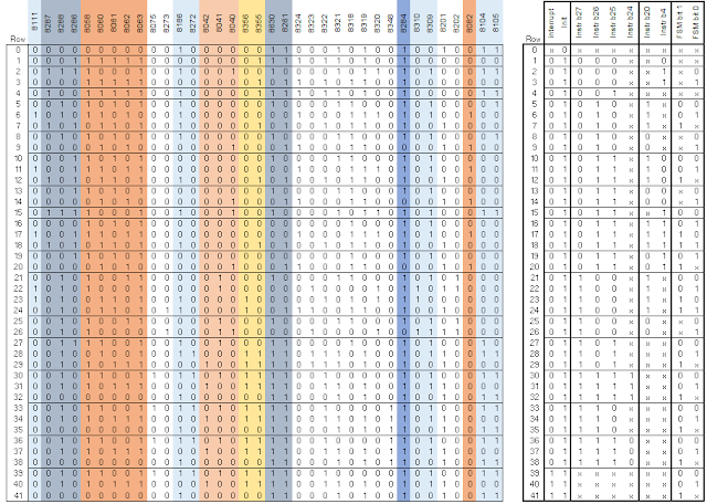
The left side of the PLA determines what the output signals will be. The presence/absence of a transistor at an individual row/column intersection determines the output on that column. The content of the left side is shown below:


(The vertical coloured stripes mark those outputs that I have reverse-engineered to date).

The output signals control other parts of the chip in a wide variety of ways. The simplest example is where output 8630 (about the middle column in the table above) which is connected directly to the chip's "opc" output pin. The opc pin indicates when the processor is fetching an instruction, so it is perhaps not surprising that this signal is set on the first cycle of most instructions in the table above. (There's interesting exceptions with the branch, software-interrupt, and co-processor instructions).

Another example is that outputs 8040, 8041, 8042 select where Read Bus A's register number is chosen from. As was described in an earlier article  these 3 bits will select between 5 different sources for these bits, and it's reassuring to scan down the columns above and note that only 5 different values are used throughout.

Preliminary analysis indicates that PLA outputs 8309, 8310 influence how the FSM input signals are generated, which is why I've I refer to them as Finite State Machine variables.

Conclusion

This analysis has given me a great insight into the way the processor's instructions are decoded and sequenced. The content of the PLA can almost be regarded as a set of instructions for a micro-instruction machine with very wide instructions (33 bits from the PLA plus 32 bits from the I-Register).

The PLA is implemented using approx. 1,100 transistors.


Sunday, January 3, 2016

Inside the armv1 - the Read Bus B, ALU Output Bus, and Address Bus

This is my fifth post describing the armv1. My earlier posts can be found here:

Ken Shirriff has also written about the arm internals here.


In this blog I'll finish describing the remaining buses - Read Bus A, the ALU Output Bus, and the Address Bus. I covered Read Bus A in an earlier post. To help set the context I reproduce the chip floorplan (but remember, this diagram incorrectly labels read bus A and read bus B the wrong way around):

Read Bus A

This should be a simple bus, as according to the floorplan, the output of the second read port of the register bank should just feed the ALU port. But it turns out it's not quite so simple:


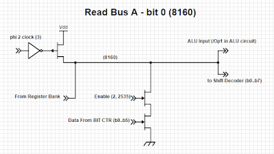
It turns out that the bottom 8 bits also feeds the Shift Decoder logic. This path is needed for the processor to implement the shift-option where a register specifies the number of bits by which the input operand is shifted.

The other surprise is that there is an option for  b0 to b5 to be sourced from the BIT CTR logic. This path is to implement the LDM/STM instructions - the first register to be loaded/saved needs to be offset from the base-register by the number of registers selected (depending on the instruction options).

Otherwise Read Bus A is like Read Bus B in that it relies on a precharge (driven by the phi 2 clock), and is inverted logic.

ALU Output Bus, Incrementer, and Address Bus

The reverse-engineered circuitry associated with the ALU Output Bus, Incrementer, and Address Bus is as follows. This is the circuit associated with bit 3:


Note that the Address Bus/Incrementer circuitry has two extra connections into the r15 (PC) register cells: an additional read signal, and an additional write signal. The new write signal operates in exactly the same way as described in my earlier post (shorts the output of one of the inverters).

The incrementer circuitry is in the centre of the diagram and comprises the 3x exclusive-nor gates, and 2-input nor gate. The control line input (7091) determines whether the circuit increments or decrements the input value (there's more about this control line below).

As with ALU described in an earlier blog, the input values to the incrementer are captured and stored by the transmission gate during the phase 1 clock time. The Carry In/Carry Out logic is slightly different for odd/even bits. This is also as described in the ALU and is to eliminate an inverter per bit and so reduce propagation delays. The Carry In signal on the first bit of the incrementer is hard-wired to 1.

Also note that the lowest 2 bits and the highest 6 bits of the PC are absent, leaving just 24 bits with circuit above. For the remaining 8 bits the incrementer isn't populated and the associated multiplexer input bits are set to zero.

The input to the incrementer is chosen by a 4-way multiplexer. The multiplexer is shown in simplified form here as the details are very similar to what we've seen already (e.g. Read Bus Decoding).

The circuit above is a little more complex than I was expecting. By experimenting with some sample programs the following becomes apparent:

  • When an instruction updates the PC (e.g. mov pc, r0), the register is updated directly through the write-select line as with any other register write; however in addition, the write value is also selected via input 1 of the multiplexer so that it can be latched by the transmission gate and be incremented ready for fetching the next instruction.
  • When a LDM/STM instruction executes (Load/Store multiple registers), the transmission gate captures the starting load/store address and the incrementer updates the address for each of the registers to be loaded/stored. Only when the last register is loaded/saved is the transmission gate re-initialised with the PC value.

The 0-input to the multiplexer varies depending on the bit, as shown in the table below.


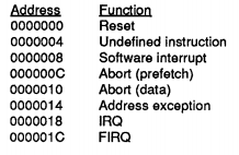
These 3x inputs come via inverters from the TRAP CTRL region of the chip and are associated with selecting the interrupt dispatch address as per the Vector Table below:


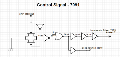
Reverse engineering of the control signal 7091 is especially puzzling. The circuit is:


This circuit really is a complex way of generating a 1 output! If this control signal is genuinely always 1 then the incrementer circuit could be substantially simpler - 2 of the exclusive nor gates could be eliminated altogether. On reviewing the chip layout itself it becomes stranger still (the image below is rotated 90 degrees):


The 0 input signals are routed a long way from the transistors themselves, even though a ground signal is right nearby, and the output, which goes nowhere, is routed in a similar area. Is it possible that part of the circuit was intended for some additional functionality which was partially implemented and then disabled at a late stage in the layout process? Any suggestions would be welcome.

Address Output Pins

The circuitry associated with the address output pins is very straightforward:

With aen_internal held low the address pins go into tri-state mode.

Conclusion

We've now reverse engineered all the remaining internal data and address buses and learnt how the incrementer circuit is used both the update the PC and to implement the LDM/STM instruction. We're reverse-engineered about 2,200 transistors in the circuits above.