
This exploration will end up covering a lot of ground - we'll find the Instruction Register and the instruction bus that feeds off it, and how data is routed in and out of the chip via the data bus. The diagram below highlights the areas of the chip we'll end up exploring.

To help navigate our way around the more complex logic, I've labelled the different areas in a zoomed in area of the top of the larger rectangle.
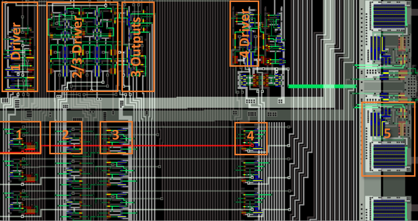
The logic for each bit associated with the Read Data Bus is laid out horizontally, and with the bits stacked on top of each other vertically - bit 31 at the top, and bit 0 at the bottom. Read Data Bus bit 31 is highlighted in red, and the areas labelled 1, 2, 3, 4 highlight the logic gates associated with bit 31. The logic is almost identical for all 32 bits, and the associated drive circuitry highlighted at the top. Also highlighted as area 5 is the logic associated with one of the data pins; we'll reverse-engineer that logic too.
We'll start by following where bit 0 of Read Bus B leads us, and then see how the remaining bits of the bus differ.

This circuit relies on stray capacitance on the bus line for its operation. During the second half of every clock cycle (when phi 2 is high) the FET in the above circuit pulls the bus line high, charging it to a high state. In the subsequent first half of the next cycle, one of three possible signals may pull the bus line low, discharging any stray capacitance. The state of the bus line is then read by either the Barrel Shifter or by Circuit 4, which processes the Data Out signal. The signal on the Read Bus is inverted logic - 0v represents a logical 1.
The signal input to the bus is one of the following:
- The output of the Read Bus B from the Register Bank, as described in the last blog.
- Data from Circuit 1, which is described below, and can be either the content of the Instruction Register, or data from the Data pins.
- Data for when the PC is being read. The armv1 architecture is such that the program counter (PC, which is R15 in the register bank), has special meanings assigned to some of its bits. These bits are not stored in the register bank, but elsewhere. Bits b0..b1 give the processor state, and bits b26..b31 are the Condition Code Register. The logic above is to read these registers at the appropriate time. This data path is in the thin vertical rectangle in the diagram above. This logic will be explored in a later post.
Complexity arises with how the circuit differs for each bit. We've already dealt with how input 3 varies. However the enable (8106) for the data from Circuit 1 also varies in a complex way. There are 5 (!) enable lines across all 32 bits of Read Bus A:

One use of this circuitry is for when a byte-read takes place - the 8 bits of data just read appear on different bit ranges depending on the lower two address bits. The enable signals above allow the valid data to put onto the Read Bus (the barrel shifter then rotates the bits to the correct position). I don't yet understand why the second and third enable signals drive just 4 bits each. The circuitry to create these 5x enable signals is in the DATA CTL area - the red rectangle at the top right of the chip:

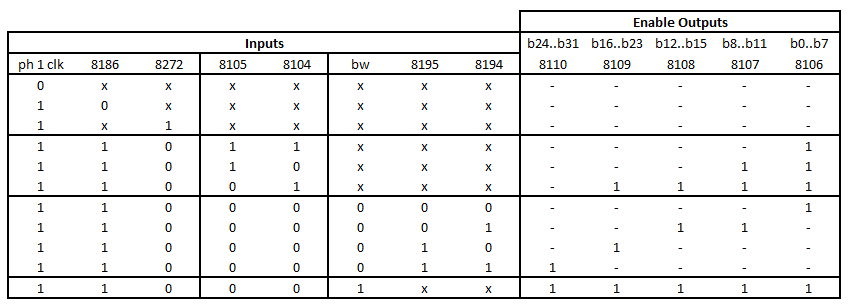
The top three rows demonstrate that the first three inputs (phi 1 clock, 8186, and 8272) must have values 1, 1, 0 respectively for there to be any output. The next three lines show the outputs for three of the possible permutations of 8105, 8104. I suspect that these are for instruction decoding:
The next 4 rows in the table are to select each byte in turn. It's almost certain 8195, 8194 are connected to Address line 1, 0.
Circuit 1 - Data In and I-Reg Multiplexing
- the first to extract the 8 bit immediate value for one variant of the Data Processing instruction.
- the second to extract the 12 bit offset for the Single Data Transfer instruction.
- the third to extract the 24 bit offset for Branch instructions.
The next 4 rows in the table are to select each byte in turn. It's almost certain 8195, 8194 are connected to Address line 1, 0.
Circuit 1 - Data In and I-Reg Multiplexing
Now that we have the circuit for the enable signal for Circuit 1 let's look at Circuit 1's internal logic, and its associated driver circuit.

So this circuit puts either Data In or I-Reg onto Read Bus B, depending on two control signal from elsewhere - signal 8111 or 8187.
The back-coupled FETs that signal 8111 feeds into warrants a little more discussion. This back-coupled FET pattern is used in many places throughout the processor, including in the ALU. This pattern appears to have two distinct uses:
Circuit 2 & 3 - The Instruction Register (or I-Reg)
The back-coupled FETs that signal 8111 feeds into warrants a little more discussion. This back-coupled FET pattern is used in many places throughout the processor, including in the ALU. This pattern appears to have two distinct uses:
- It can be used ax a multiplexer, as shown further down in the same circuit.
- Or in this case it can be used as a "latch". Whilst the phi 1 clock is high both FETs are turned on and the 8111 signal passes through the FETs to the input to the AND gate. When the phi 1 clock goes low the two FETs are turned off and the input to the AND is left floating. The stray capacitance of the node means the voltage will be maintained for a short period, until any charge is dissipated through leakage. The capacitance must be large enough, and the leakage small enough, for the correct logic value to be maintained until the next clock cycle. This is presumably why the processor has a maximum clock cycle time of around 10 microseconds; any longer and the correct value would not be held.
Circuit 2 & 3 - The Instruction Register (or I-Reg)
The Instruction -Register logic is as follows:

The Instruction Register itself is the cross-coupled inverter on the right, although it's difficult to see with the FET multiplexers at each inverter's input. The pair of multiplexers that feed the lower cross-coupled inverter determine whether the register maintains its current (looped back) state or whether it is updated from a delayed copy of Read D0. Input 8187 selects which multiplexer is selected. The 3x input signals that control this circuit will be explored subsequently, but a quick look shows that input 4585 is derived from the opc pin, which indicates that the processor is fetching an instruction, so we're definitely on the right track!
The I-Reg outputs form a bus that runs right across the chip, pretty much as illustrated in the floorplan at the beginning of this blog. However, there are a few exceptions:
Circuit 4 - Data Out (DOUT) Processing

The Instruction Register itself is the cross-coupled inverter on the right, although it's difficult to see with the FET multiplexers at each inverter's input. The pair of multiplexers that feed the lower cross-coupled inverter determine whether the register maintains its current (looped back) state or whether it is updated from a delayed copy of Read D0. Input 8187 selects which multiplexer is selected. The 3x input signals that control this circuit will be explored subsequently, but a quick look shows that input 4585 is derived from the opc pin, which indicates that the processor is fetching an instruction, so we're definitely on the right track!
The I-Reg outputs form a bus that runs right across the chip, pretty much as illustrated in the floorplan at the beginning of this blog. However, there are a few exceptions:
- A few outputs are not connected. These are bits 25, 26, and 27.
- There are 6x I-Register outputs that are fed from the opposite side of the cross-coupled inverters. These are bits 4 (7887), 20 (7888), 24 (7889), 25 (7890), 26 (7891), 27 (7892). These all feed into inverters and the inverted outputs join the other I-Reg signal bus. The inverters are in the area marked "3 Outputs" in the earlier image.
Circuit 4 - Data Out (DOUT) Processing
The final circuit connected to Read Bus A is the Data Out (DOUT) processing logic which in the area marked as "4" in the earlier image:

This logic interfaces the Read Bus with the processor's data bus. Normally all 32 bits of the Read Bus are presented to the data pins; however during a byte-write, the data in the lowest byte is also presented on 3 the upper bytes too.
The logic for the 8 lowest bits is the identical, and passes the signal to the other bits via an 8-bit wide bus, and also towards the Read/Write pin on nbus signals.
The logic for bits 8-31 is also identical. The signal is multiplexed in from either the Read Bus B input or from the 8-bit wide bus fed by bits 0..7. The bw (byte not word) input signal selects between the two inputs. We've already encountered the bw input signal in the Read Bus B decoding logic.
Circuit 5 - Data Lines 0 to 31
The final circuit to explore is associated with each data line, and is highlighted in the diagram above as circuit 5.

This circuit identifies the destination of the nbus signal referred to in the Data Out logic, and the source of the Read D0 signal that's seen in the Data In logic, and the Instruction Register logic.
We also see the R/W pin, and the dbe (data bus enable) pin having a part to play in the logic.
Conclusion
We have finally completed our exploration of the Read Bus B logic, and in the process identified the Instruction Register (I-Reg) and how data is read and written to the data pads. We've also seen some of the complexities of dealing with byte/word reads and writes and how reading r15 (the PC) is a special case. Around 2,200 transistors are used to implement these circuits.
To have located the Instruction Register is an important step forward as it is its content that drives much of the processor's control logic. But all that is for future blog posts.
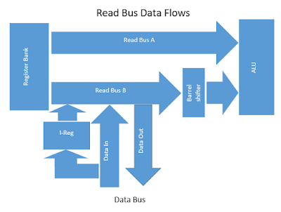
But let's not get lost in the details. Overall, the circuitry described in this post accomplishes some simple routing, which are summarised in the diagram below, which is a little more explicit than the floorplan diagram above. Yes, there are extra details that aren't shown in the diagram, but it helps to keep this overview in mind too.
We also see the R/W pin, and the dbe (data bus enable) pin having a part to play in the logic.
Conclusion
We have finally completed our exploration of the Read Bus B logic, and in the process identified the Instruction Register (I-Reg) and how data is read and written to the data pads. We've also seen some of the complexities of dealing with byte/word reads and writes and how reading r15 (the PC) is a special case. Around 2,200 transistors are used to implement these circuits.
To have located the Instruction Register is an important step forward as it is its content that drives much of the processor's control logic. But all that is for future blog posts.
But let's not get lost in the details. Overall, the circuitry described in this post accomplishes some simple routing, which are summarised in the diagram below, which is a little more explicit than the floorplan diagram above. Yes, there are extra details that aren't shown in the diagram, but it helps to keep this overview in mind too.

No comments:
Post a Comment