Today, we'll explore the area that I labelled PLA2 in an earlier article:

We know that PLA2 is an important part of the chip, partly because a substantial portion of silicon has been allocated for it, and partly because in our reverse-engineering efforts we have already found lots of signals tracing back to it. I had been putting off looking at it because I feared it would be a "sea of logic" and contain lots of ad-hoc and difficult to understand calculations. However my interest was piqued when by chance I noticed whilst stepping through various instructions that only a single row within the PLA was active at a time - clearly there was more structure to the logic than I was expecting. It became even more interesting when I realised that the main inputs to the PLA were the "special" I-Reg signals that I'd found earlier my earlier post: bits 4, 20, 24, 24, 26, 27 of the I-Reg are separately wired directly (and only) to the PLA input!
Before we embark any further, let's zoom in on the PLA layout:

Ten input signals arrive at the top right and the signals, and their inverted versions, feed the 20x vertical columns on the right and intersect 42 horizontal rows. At each intersection there can be one of three options:
- A transistor for the non-inverted signal, OR
- A transistor for the inverted signal, OR
- No transistor
By default the horizontal line is pulled high, and if any transistor on any vertical intersections is turned on, the horizontal line is pulled low. The way the transistors are cunningly placed ensures that only one horizontal line is pulled low at any time.
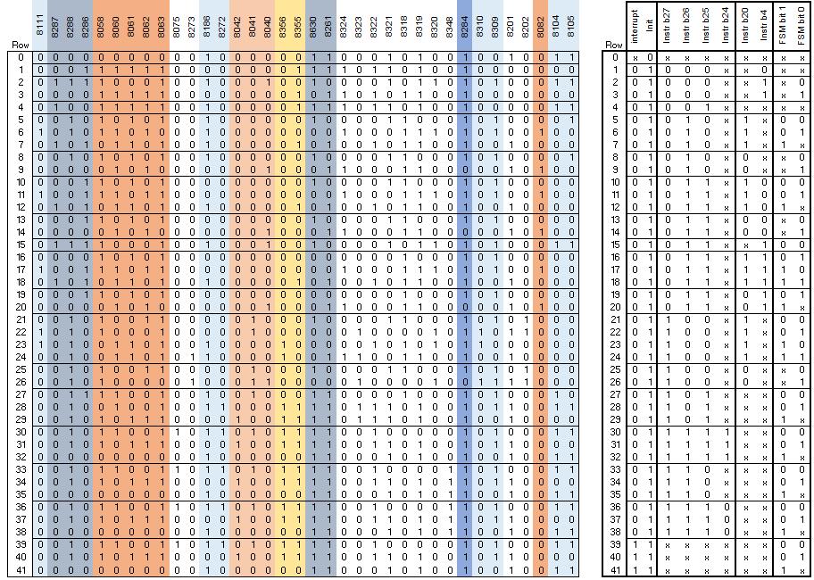
By knowing the source of at least some of the inputs and working through where the transistors are placed it was possible to build up the logic table below:

On the left of the table is where the transistors are in the layout. An 'x' marks where no transistor was fitted and is a "don't care" in the decoding. On the right I've broken out the logic represented by the transistor placements in a step-by step manner:
The first column on the right shows only the top row is active when the "Init" input is 0; every other column input on this row is "don't care". All remaining rows require the "Init" input to be 1 in order to be selected.
The second column breaks down the case of "Init" = 0 - in this case the Interrupt signal divides the remaining columns into two sections rows 1-38 for Interrupt = 0, and rows 39-41 for Interrupt = 1.
Note that I've made a best-guess at the names for these first two input bits based on what signals are present during experiments with reset and interrupt processing.
The third column divides the input into 7 major instruction types, depending on the "special" I-Reg inputs that I mentioned earlier. The following columns then break the instructions into finer and finer categories.
By studying the table it's possible to see how the decoding options have been constructed so that every input combination on ever decodes to a single output - brilliant.
You'll notice that most instructions decode to several rows in the table, with just input signals FSM 0, 1 differentiating them (e.g. LDM decodes to lines 21-24). Again the signal names FSM 0, 1 are mine and allude to the operation appearing to be not unlike a Finite State Machine. Each row is a different stage/cycle in the instruction's execution. Most instructions simply step through each row on successive clock cycles and therefore the number of rows in the table above shows how long it takes each instruction to execute. There is one exception to this, which is for the LDM/STM instruction pair. These instructions load/store between 1 to 16 registers to memory, depending on a 16 bit bit-pattern. In these cases the processor stays in a single state "looping" until all registers have been loaded/saved. This can be seen in the animation below which shows the execution of an LDM instruction which loads 8 registers.

On the first cycle it "executes" row 21, then row 22, then loops on row 23 for each register, and finally "executes" row 24 before the processor moves to the next instruction.
There is a huge amount that can be learnt from studying the decoding table above:
First, only two instruction variants execute in a single cycle; many take 2 or 3 cycles.
Second, it's surprising to see that Coprocessor instructions are being decoded; this functionality is not otherwise present on this chip and only introduced on its successor, the VL86C010 (more details on this chip are available here).
Third, rows 15-20 decode some instructions that are not documented. What's more, this part of the "instruction space" is explicitly declared as "undefined(reserved)" on page 2-49 of the VL86C010 documentation. Perhaps with some more reverse-engineering we'll be able to confirm what these instructions do on this chip.
The left side of the PLA determines what the output signals will be. The presence/absence of a transistor at an individual row/column intersection determines the output on that column. The content of the left side is shown below:
The output signals control other parts of the chip in a wide variety of ways. The simplest example is where output 8630 (about the middle column in the table above) which is connected directly to the chip's "opc" output pin. The opc pin indicates when the processor is fetching an instruction, so it is perhaps not surprising that this signal is set on the first cycle of most instructions in the table above. (There's interesting exceptions with the branch, software-interrupt, and co-processor instructions).
Another example is that outputs 8040, 8041, 8042 select where Read Bus A's register number is chosen from. As was described in an earlier article these 3 bits will select between 5 different sources for these bits, and it's reassuring to scan down the columns above and note that only 5 different values are used throughout.
Preliminary analysis indicates that PLA outputs 8309, 8310 influence how the FSM input signals are generated, which is why I've I refer to them as Finite State Machine variables.
Conclusion
This analysis has given me a great insight into the way the processor's instructions are decoded and sequenced. The content of the PLA can almost be regarded as a set of instructions for a micro-instruction machine with very wide instructions (33 bits from the PLA plus 32 bits from the I-Register).
The PLA is implemented using approx. 1,100 transistors.
How do the 20 horizontal rows manage both high and low? The P-FETs at the right side is always active, so does it just rely on more N-FETs being active (and/or the N-FETs being stronger) in the 10x20 block when that row needs to be low?
ReplyDeleteAnd doesn't that waste a considerable amount of power?
DeleteYou're right - it's a static pullup, both for the left-hand block and the right-hand, formed with weak always-on PMOS transistors. A bit like the design style of an NMOS chip like 6502 or 6800, and whenever an output should be low it will draw static power. Almost all the outputs of the input block, the right one, will be low in a given clock cycle.
DeleteThe only other transistor-efficient approach in CMOS would be a clocked design.
How do the 20 horizontal rows manage both high and low? The P-FETs at the right side is always active, so does it just rely on more N-FETs being active (and/or the N-FETs being stronger) in the 10x20 block when that row needs to be low?
ReplyDeleteAccording to an old ARM2 manual I've got kicking around, the "shift amount is in a register" version of the LDM/STM instructions wasn't considered a reserved instruction in the ARM1. There's a series of changes noted in the manual, ARM2 vs. ARM1, and that is one of the ones called out. That might explain why that grouping of reserved instructions is actually decoded in the original ARM1.
ReplyDelete