Architectural descriptions of the armv1 tell us that the chip contains a bank of 25 registers, each 32 bits wide. Of these 25 registers, only 16 are visible to the programmer at a time and are referenced in the instructions as registers number 0 to 15, with register 15 being the Program Counter or PC. The extra registers are there to support the four modes that the processor runs in - supervisor, interrupt, fast interrupt, and user mode. For instance the fast interrupt mode has it's own copy of five of the registers - r10, r11, r12, r13, and r14.
We also know from the architecture that the register bank has two read buses and one write bus. We also know from my last blog that one of the read buses goes directly to the ALU, and that the output of the ALU goes to the write bus. This is nicely illustrated in the following block diagram:

(Please note that it has recently been noticed that this historical diagram has incorrectly labelled read bus A and read bus B the wrong way around; all other documents name them the other way around. This blog series has therefore been updated to label the buses correctly)
Now that we have a bit more context it's time to zoom into the details on the chip, starting at the lowest level of detail - a single bit. Each of the 32 bits of all 25 registers is the same - a cross-coupled inverter, with three separate select lines. The silicon layout is as follows:
Now that we have a bit more context it's time to zoom into the details on the chip, starting at the lowest level of detail - a single bit. Each of the 32 bits of all 25 registers is the same - a cross-coupled inverter, with three separate select lines. The silicon layout is as follows:

The equivalent circuit is:
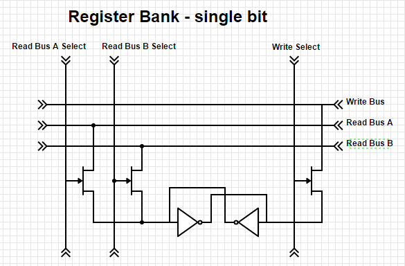
What is interesting about this circuit is that the write circuit shorts the output of one of the inverters! The write select transistor and the Write Bus driver transistors are comparatively large, and much larger than the transistors in the inverter, ensuring that they will "win". Once the inverter's output has been overpowered, the cross-coupled inverters will quickly transition to the new state, ensuring that the short condition lasts only a very short time. The 3x select lines per register run vertically, as shown in the chip detail above. Likewise, the 32 bits per register (x3, one for each bus) run horizontally.
Select Line Decoding
The three select lines for each of the 25 register are generated by the decode circuitry above the register bank. The similarities in the decoding between the three select lines, and between the registers is visually very apparent:

I'll start by describing the decode circuitry for Read Bus B, and later show how the decoding for Read Bus A and the Write Bus differ only slightly. There are two steps to the decoding process, first decoding the register number, and then the processor state/mode. Decoding by the register number is via the following circuit:

I've laid out the diagram so such that the horizontal lines match the chip layout. The b3, b2, b1, b0 inputs select the register; the logic to set these values will be reverse-engineered in a later blog. Note that each input to the NAND gate has only one connection (not 2 as shown in the diagram) - it will be connected either to an input bit or its inverse.
The subsequently decoding based on processor state/mode is as follows:
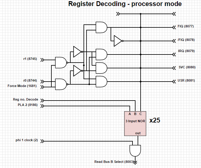
Again, the diagram is laid out so that the horizontal lines match the chip layout. The C NOR input is connected to just one of the 5 horizontal lines that select the processor modes. The output of the AND gate feeds to the register array. Note that the horizontal lines also feed the Read Bus B and Write Select logic.
The settings for the 25x sets of decoders are summarised in the table below:

The decoding for the Read Bus A and Write Select is very similar. The registers selection logic is almost identical, with only the source of the b3..b0 input signals differing, as shown in the table below:

There are only minor differences in the processor state/mode decoding.The updated circuits are shown below:

Note that the write decoding is driven from the phi 2 clock, whereas both sets of read decoding is driven from the phi 1 clock. We'll need to pick up on the timing-related aspects later.
Finally, r15, the Program Counter, has some slight variations from the above; these need to be investigated later.
Conclusion
We now have a complete breakdown of the register bank and how the three ports - two read, and one write - operate. A little over 6,000 transistors are needed for its implementation. There are very few external signals that control its operation, and these will be clarified later as we continue with the reverse engineering.
No comments:
Post a Comment