
Let's start with Read Bus B, bit 3:

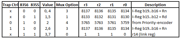
The result, which includes all 4 bits can be summarised in the table below:

Read Bus A is also fed from a 5 way input multiplexer, but the selection logic is much simpler:
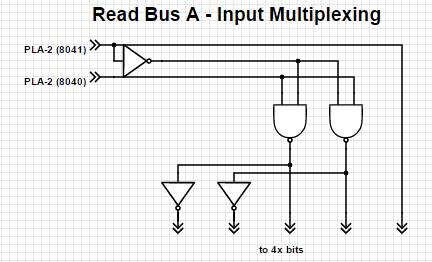
Two of the multiplexer "channels" comprise N-FETs (those driven by the inverters in the circuit above), with the and remaining "channels" constructed of P-FETs, The multiplexing operation across all 4 bits is:

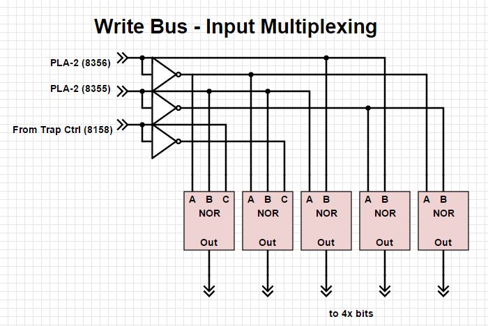
The Write Bus is fed from a 5 way input multiplexer too, with the following circuit:
The results of it's multiplexing across all 4 bits is:
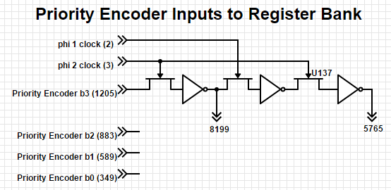
So the 4 bit wide priority-encoder signal is delayed slightly before being used as input the Read Bus A multiplexer and Write Bus multiplexer. The circuit for the remaining 3 of the 4 bits is identical.
Conclusion
This analysis has significantly clarified our understanding of how the registers selection works - the PLA-2 outputs control which fields from the Instruction Register are used to select the 3x register bank inputs/outputs. There are a few exceptions where r14 or r15 is selected or the data from the priority encoder is used.
Only approximately 150 transistors are used to implement these circuits.
No comments:
Post a Comment