- Inside the ALU of the armv1 - the first ARM microprocessor
- Inside the armv1 Register Bank
- Inside the armv1 Read Bus
- Inside the armv1 Register Bank - register selection
Ken Shirriff has also written about the arm internals here.
In this blog I'll finish describing the remaining buses - Read Bus A, the ALU Output Bus, and the Address Bus. I covered Read Bus A in an earlier post. To help set the context I reproduce the chip floorplan (but remember, this diagram incorrectly labels read bus A and read bus B the wrong way around):

This should be a simple bus, as according to the floorplan, the output of the second read port of the register bank should just feed the ALU port. But it turns out it's not quite so simple:
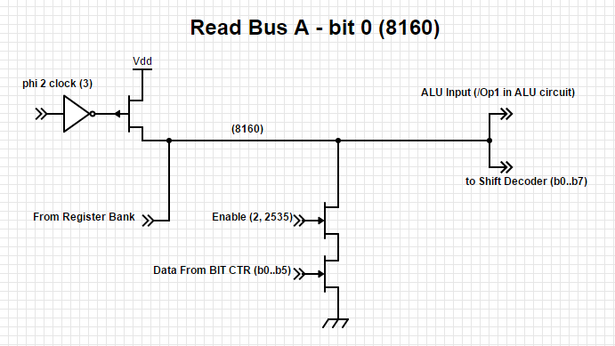
It turns out that the bottom 8 bits also feeds the Shift Decoder logic. This path is needed for the processor to implement the shift-option where a register specifies the number of bits by which the input operand is shifted.
The other surprise is that there is an option for b0 to b5 to be sourced from the BIT CTR logic. This path is to implement the LDM/STM instructions - the first register to be loaded/saved needs to be offset from the base-register by the number of registers selected (depending on the instruction options).
Otherwise Read Bus A is like Read Bus B in that it relies on a precharge (driven by the phi 2 clock), and is inverted logic.
ALU Output Bus, Incrementer, and Address Bus
The reverse-engineered circuitry associated with the ALU Output Bus, Incrementer, and Address Bus is as follows. This is the circuit associated with bit 3:

Note that the Address Bus/Incrementer circuitry has two extra connections into the r15 (PC) register cells: an additional read signal, and an additional write signal. The new write signal operates in exactly the same way as described in my earlier post (shorts the output of one of the inverters).
The incrementer circuitry is in the centre of the diagram and comprises the 3x exclusive-nor gates, and 2-input nor gate. The control line input (7091) determines whether the circuit increments or decrements the input value (there's more about this control line below).
As with ALU described in an earlier blog, the input values to the incrementer are captured and stored by the transmission gate during the phase 1 clock time. The Carry In/Carry Out logic is slightly different for odd/even bits. This is also as described in the ALU and is to eliminate an inverter per bit and so reduce propagation delays. The Carry In signal on the first bit of the incrementer is hard-wired to 1.
Also note that the lowest 2 bits and the highest 6 bits of the PC are absent, leaving just 24 bits with circuit above. For the remaining 8 bits the incrementer isn't populated and the associated multiplexer input bits are set to zero.
The input to the incrementer is chosen by a 4-way multiplexer. The multiplexer is shown in simplified form here as the details are very similar to what we've seen already (e.g. Read Bus Decoding).
The circuit above is a little more complex than I was expecting. By experimenting with some sample programs the following becomes apparent:
- When an instruction updates the PC (e.g. mov pc, r0), the register is updated directly through the write-select line as with any other register write; however in addition, the write value is also selected via input 1 of the multiplexer so that it can be latched by the transmission gate and be incremented ready for fetching the next instruction.
- When a LDM/STM instruction executes (Load/Store multiple registers), the transmission gate captures the starting load/store address and the incrementer updates the address for each of the registers to be loaded/stored. Only when the last register is loaded/saved is the transmission gate re-initialised with the PC value.
The 0-input to the multiplexer varies depending on the bit, as shown in the table below.

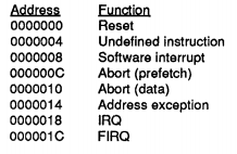
These 3x inputs come via inverters from the TRAP CTRL region of the chip and are associated with selecting the interrupt dispatch address as per the Vector Table below:
Reverse engineering of the control signal 7091 is especially puzzling. The circuit is:

This circuit really is a complex way of generating a 1 output! If this control signal is genuinely always 1 then the incrementer circuit could be substantially simpler - 2 of the exclusive nor gates could be eliminated altogether. On reviewing the chip layout itself it becomes stranger still (the image below is rotated 90 degrees):

The 0 input signals are routed a long way from the transistors themselves, even though a ground signal is right nearby, and the output, which goes nowhere, is routed in a similar area. Is it possible that part of the circuit was intended for some additional functionality which was partially implemented and then disabled at a late stage in the layout process? Any suggestions would be welcome.
Address Output Pins
The circuitry associated with the address output pins is very straightforward:

Conclusion
We've now reverse engineered all the remaining internal data and address buses and learnt how the incrementer circuit is used both the update the PC and to implement the LDM/STM instruction. We're reverse-engineered about 2,200 transistors in the circuits above.
No comments:
Post a Comment